
Placing components | Cutting tracks | Planning a layout | Example plan
Also see: Breadboard | PCB | Types of Circuit Board
|
| Stripboard circuit (copper tracks side) |
Stripboard is used to make up permanent, soldered circuits. It is ideal for small circuits with one or two ICs (chips) but with the large number of holes it is very easy to connect a component in the wrong place. For large, complex circuits it is usually best to use a printed circuit board (PCB) if you can buy or make one.
Stripboard requires no special preparation other than cutting to size. It can be cut with a junior hacksaw, or simply snap it along the lines of holes by putting it over the edge of a bench or table and pushing hard, but take care because this needs a fairly large force and the edges will be rough. You may need to use a large pair of pliers to nibble away any jagged parts.
Avoid handling stripboard that you are not planning to use immediately because
sweat from your hands will corrode the copper tracks and this will make soldering
difficult. If the copper looks dull, or you can clearly see finger marks, clean
the tracks with fine emery paper, a PCB rubber or a dry kitchen scrub before
you start soldering.
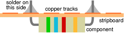 Components are placed on the non-copper side, then the stripboard is turned over
to solder the component leads to the copper tracks.
Components are placed on the non-copper side, then the stripboard is turned over
to solder the component leads to the copper tracks.
Stripboard layouts are shown from the component side, so the tracks are out of sight under the board. Layouts are normally shown with the tracks running horizontally across the diagram.
Placing components on stripboard requires care. The large number of holes means it is very easy to make a mistake! For most small circuits the best method is to very carefully place the chip holder(s) in the correct position and solder in place. Then you can position all the other components relative to the chip holder(s).
Minor position errors left and right will not usually be a problem because the component will still be connected to the correct tracks. However, up and down position errors must be avoided because just one hole too high or too low will connect the component to the wrong track and therefore the wrong part of the circuit.
Some people like to label the holes with letters (up/down) and numbers (across) to
give each hole a 'grid reference' but this still requires careful counting of holes.
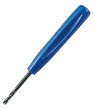 |
| Track cutter Photograph © Rapid Electronics |
Places where the tracks must be broken are usually shown with a cross (X). The cuts are made on the underside (copper side) so extra care is needed to identify the correct hole. It is best to cut the track after soldering because the solder joints will make it easier to identify the correct position.
Place the track cutter on the correct hole and twist it to and fro using moderate force.
The aim is to break the copper track, not drill a hole through the board!
Inspect the cut closely to ensure there is no fine thread of copper left across the break,
because even the tiniest piece will conduct.
Collect all the parts you will be using in the circuit so you can use a piece of stripboard to work out the minimum space they require. For some components (such as chip holders) the space required is fixed, but for others you can increase the space to obtain a better layout. For example most resistors require at least 3 hole-spacings if they are to lie flat on the board, but they can easily span across a greater distance.
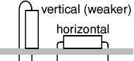 If necessary resistors can be mounted vertically between adjacent tracks (0.1"
spacing) as shown in the diagram. This arrangement can help to produce a simpler
layout but the tracks are more likely to be damaged if the resistor is knocked.
If you are designing a stripboard layout for a serious long-term purpose it is
best to mount all resistors horizontally.
If necessary resistors can be mounted vertically between adjacent tracks (0.1"
spacing) as shown in the diagram. This arrangement can help to produce a simpler
layout but the tracks are more likely to be damaged if the resistor is knocked.
If you are designing a stripboard layout for a serious long-term purpose it is
best to mount all resistors horizontally.
Plan the layout with a pencil and paper (or on computer if you have suitable software)
and check your plan very carefully against the circuit diagram BEFORE you attempt to
solder any part of the circuit. The best way to explain the planning process is by
example, so there is a step-by-step example to follow below.
| The Planning Sheet is supplied as a PDF file, to view and print it you need an Acrobat Reader which may be downloaded free for Windows, Mac, RISC OS, or UNIX/Linux computers. If you are not sure which type of computer you have it is probably Windows. |
Working 'real size' on a 0.1" grid makes it easy to allow the correct space for
components, but you will need to draw very neatly. If you prefer to work at an enlarged
scale you can use a piece of stripboard for measuring component sizes in 'number of holes'.
The stripboard tracks are horizontal in all the diagrams.
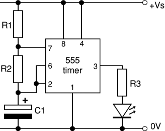 |
| Astable Circuit Diagram |
The LED flashes at a rate determined by the resistors R1 and R2 and the capacitor C1.
R1 must be at least 1k![]() and both R1 and R2 should not be more than 1M
and both R1 and R2 should not be more than 1M![]() .
To select a value for the LED resistor R3 please see the
LEDs page.
.
To select a value for the LED resistor R3 please see the
LEDs page.
LED on time: Tm = 0.7 × (R1 + R2) × C1
LED off time: Ts = 0.7 × R2 × C1
T = Tm + Ts = 0.7 × (R1 + 2R2) × C1
Frequency (flashes per second), f = 1/T
Tm and Ts are about equal if R2 is much larger than R1.
For further information please see 555 astable.
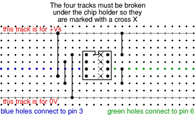
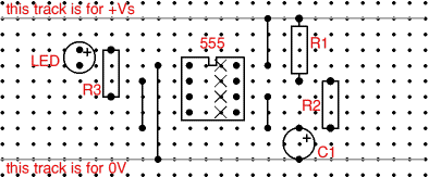
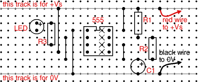
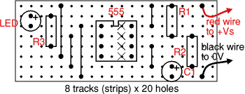
Connections which do not involve the chip are made using an unused track. For example resistor R3 and the LED are connected by an unused track above the chip.
Watch for alternative arrangements using the links you have already made. For example the LED needs to connect to 0V but it is a long stretch to the 0V track. It is easier to connect the LED to the same track as pin 1 of the chip because that track is already connected to 0V by a wire link.
Resistor R2 needs to connect from pin 7 to pin 6 and it could do this directly by mounting it vertically. However, it has been connected from pin 7 to the track used to link pins 2 and 6, the extra space this gives allows R2 to lie horizontally on the board.
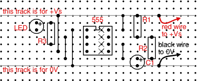
Unused tracks above and below the chip have been eliminated in the example. This affected two components, resistor R1 and capacitor C1, but both will still fit in the reduced space. The plan could be compressed a little further by moving components and links closer to the chip horizontally but this has not been done.
It is tempting to rush straight into soldering the circuit, but do check your plan carefully first. It is much easier to correct errors on the plan than it is to correct to correct them on the soldered board!
| Flashing LED Circuit
|
|